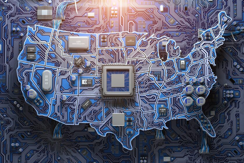
In the fast-paced world of electronics design and manufacturing, the ability to rapidly prototype and iterate is crucial. The emergence of 3D printed PCB prototyping has significantly transformed this landscape, enabling faster iterations and reducing costs. This technological advancement holds particular promise for industries ranging from medical device manufacturing to aerospace and defense.
The Traditional PCB Prototyping Process
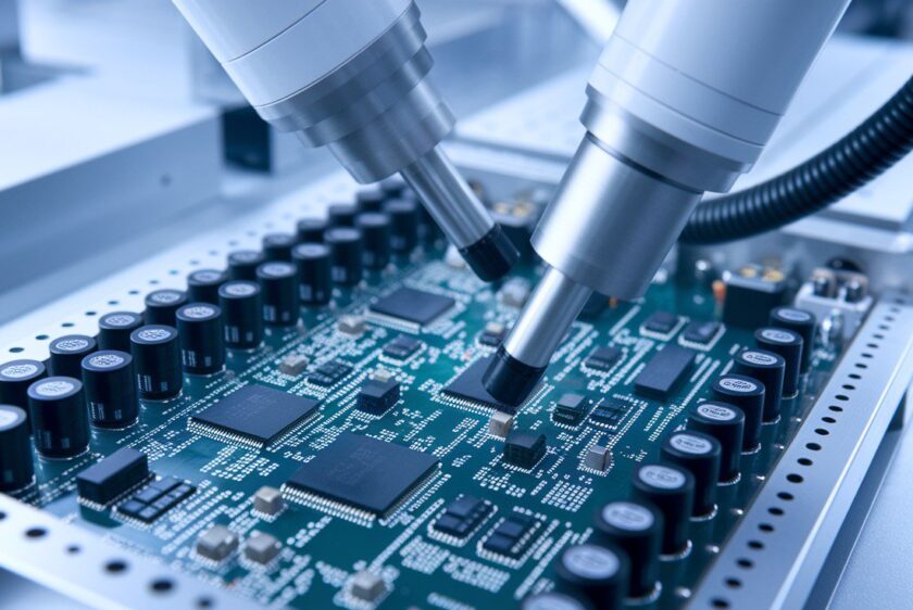
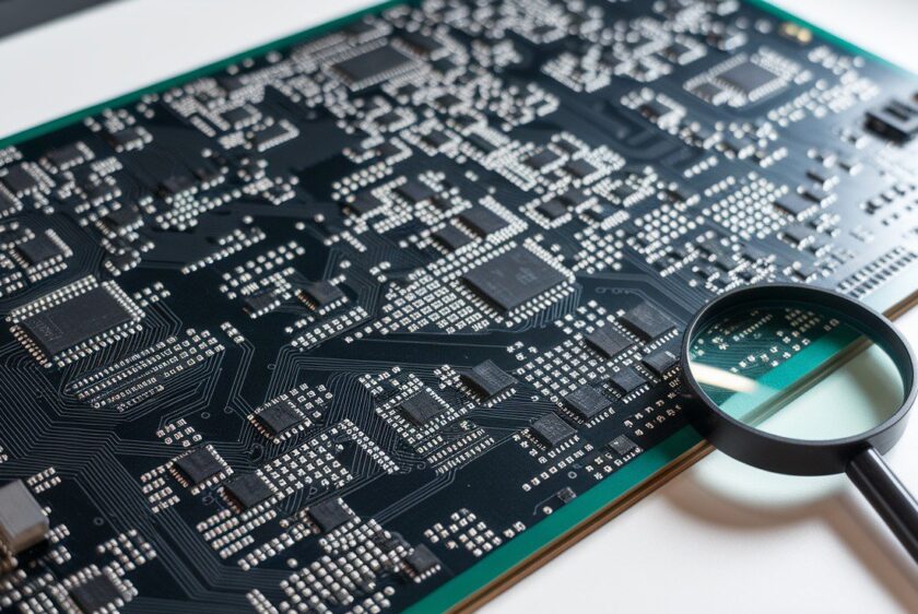
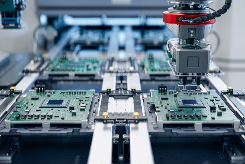
Historically, PCB prototyping has been a time-consuming and expensive process. Traditional methods involve multiple steps including designing the layout, fabricating the board using photolithography or etching techniques, assembling components, and testing. Each iteration can take weeks or even months, resulting in high costs and delayed project timelines.
The Advent of 3D Printed PCB Prototyping
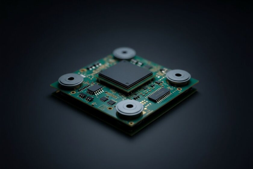
The introduction of 3D printing technology into PCB prototyping has revolutionized this process. By leveraging additive manufacturing techniques, designers can now create complex multi-layered PCBs with conductive materials directly from digital designs. This method offers several key advantages:
Speed and Efficiency
One of the most significant benefits of 3D printed PCB prototyping is the dramatic reduction in production time. What once took weeks can now be accomplished in a matter of hours or days. For industries where time-to-market is critical—such as consumer electronics developers or telecommunications equipment providers—this speed can provide a substantial competitive edge.
Cost Reduction
Traditional PCB fabrication involves costly setup fees for each iteration due to tooling changes and material wastage. In contrast, 3D printing minimizes these expenses by eliminating the need for physical tooling. Additionally, it allows for on-demand production without large minimum order quantities, making it particularly advantageous for small-scale projects or custom designs often needed by industrial electronics manufacturers and wearable technology companies.
Design Flexibility
Additive manufacturing enables unprecedented design flexibility that traditional methods cannot match. Complex geometries, embedded components, and customized features are more easily achievable with 3D printed PCBs. This capability is invaluable for sectors like biotechnology equipment firms and optical & photonics equipment manufacturers who require intricate designs tailored to specific applications.
Rapid Iteration Cycles
The ability to quickly produce prototypes means that engineers can test multiple iterations in rapid succession. This iterative approach leads to more refined end products as issues can be identified and resolved early in the development cycle. For defense contractors and automotive electronics suppliers dealing with stringent performance standards, this iterative refinement process is essential.
Applications Across Diverse Industries
The impact of 3D printed PCB prototyping spans various industries:
- Medical Device Manufacturers: Accelerates development cycles for life-saving devices.
- Military Equipment Producers: Enhances precision in designing robust communication systems.
- Aerospace Industry Suppliers: Facilitates lightweight yet durable electronic components.
- Consumer Electronics Developers: Speeds up innovation while reducing costs.
- Renewable Energy Tech Companies: Enables efficient design of smart grid technologies.
Challenges and Future Prospects
While the advantages are clear, there are still challenges to address before widespread adoption becomes feasible across all sectors:
- Material Limitations: Current conductive inks used in 3D printing may not yet match traditional materials' electrical properties.
- Resolution Constraints: Achieving fine resolution necessary for high-density interconnects remains an ongoing challenge.
- Standardization Issues: Lack of industry-wide standards for 3D printed PCBs could hinder interoperability between different systems.
However, continuous advancements in materials science and printing technologies promise to overcome these hurdles soon enough. As research progresses towards improving conductivity materials and enhancing print resolutions, we anticipate broader acceptance within industries such as satellite technology developers or AI hardware firms seeking cutting-edge solutions.
Conclusion
The advent of 3D printed PCB prototyping represents a paradigm shift within electronic product design realms—from medical devices to aerospace technologies—ushering faster iterations at lower costs than ever before possible through traditional means alone. While challenges remain on this transformative journey towards full-scale implementation across diverse sectors; ongoing innovations hold immense potential unlocking new frontiers shaping future landscapes where rapid prototyping becomes synonymous seamless efficiency driving unparalleled progress forward!